| CPC H01L 29/7813 (2013.01) [H01L 21/26513 (2013.01); H01L 21/765 (2013.01); H01L 29/0696 (2013.01); H01L 29/1095 (2013.01); H01L 29/407 (2013.01); H01L 29/66734 (2013.01)] | 18 Claims |
|
1. A power MOSFET device, comprising:
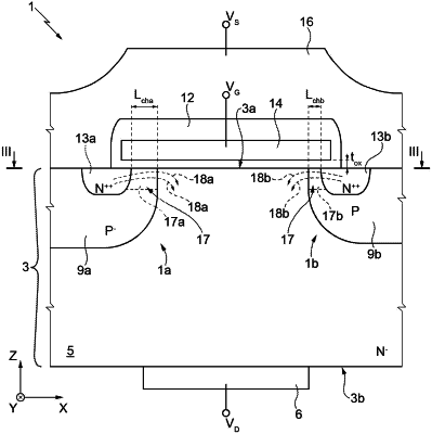
a semiconductor body having a first surface extending along a first direction and a second surface opposite the first surface, the semiconductor body including an active area, the active area including:
a first body region having a first conductivity type and a first conductivity value;
a second body region having the first conductivity type and a second conductivity value higher than the first conductivity value;
a first source region extending in the semiconductor body from the first surface, the first source region disposed adjacent to the first body region, and having a second conductivity type different from the first conductivity type;
a second source region extending in the semiconductor body from the first surface, the second source region disposed adjacent to the second body region, and having the second conductivity type;
an insulated-gate region extending within or over the active area and having a first portion facing the first body region and the second body region and a second portion facing the first source region and the second source region;
a drain region having the second conductivity type and extending in the semiconductor body from the second surface;
a first channel region within the first body region, between the first source region and the drain region; and
a second channel region within the second body region, between the second source region and the drain region,
wherein the first channel region has a first channel length along the first direction, and the second channel region has a second channel length along the first direction that is smaller than the first channel length, and
wherein the first body region, the first source region, the drain region, the first portion of the insulated-gate region, and the first channel region form a first device portion having a first threshold voltage, and the second body region, the second source region, the drain region, the second portion of the insulated-gate region, and the second channel region form a second device portion having a second threshold voltage higher than the first threshold voltage.
|