| CPC H01L 29/7813 (2013.01) [H01L 29/0634 (2013.01); H01L 29/0696 (2013.01); H01L 29/4236 (2013.01); H01L 29/66734 (2013.01)] | 19 Claims |
|
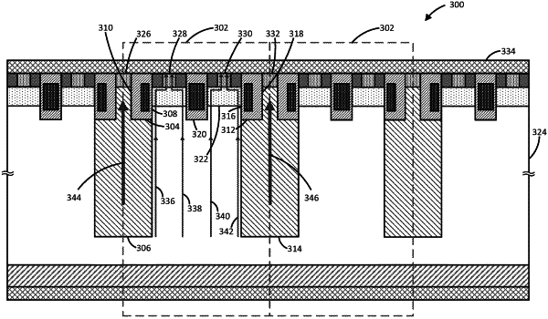
15. A power semiconductor device including a plurality of unit cells, each unit cell comprising:
a first trench gate provided in a first pillar, the first trench gate having a first side aligned with a vertical edge of the first pillar and a second side facing an interior of the first pillar;
a second trench gate provided in a second pillar, the second trench gate having a first side aligned with a vertical edge of the second pillar and a second side facing an interior of the second pillar, the first and second pillars being adjacent pillars;
a third trench gate provided between the first and second trench gates, the third trench gate extending into a drift region; and
first, second, third, and fourth heavily doped regions making Ohmic contacts with an electrode, the first heavily doped region being provided in the first pillar, the second heavily doped region provided between the first and third trench gates, the third heavily doped region provided between the second and third trench gates, and the fourth heavily doped region provided within the second pillar.
|