| CPC H01L 29/7786 (2013.01) [H01L 29/2003 (2013.01); H01L 29/402 (2013.01); H01L 29/66462 (2013.01)] | 20 Claims |
|
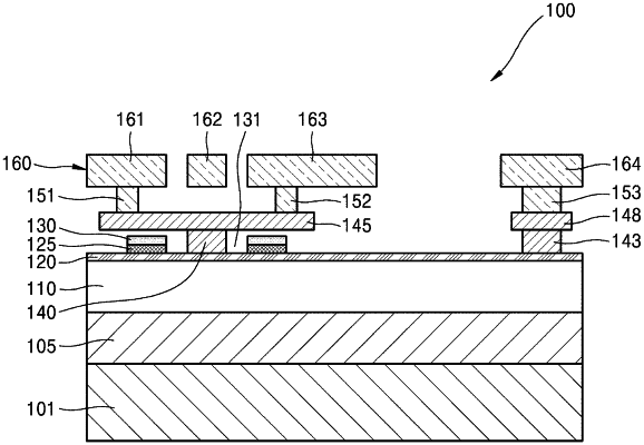
1. A high electron mobility transistor (HEMT) comprising:
a channel layer including a group III-V compound semiconductor;
a barrier layer on the channel layer, the barrier layer including the group III-V compound semiconductor;
a gate electrode on the barrier layer;
a source electrode over the gate electrode;
a drain electrode spaced apart from the source electrode; and
a metal wiring layer including a gate wiring connected to the gate electrode, a source field plate connected to the source electrode, and a drain field plate connected to the drain electrode,
the gate wiring, the source field plate, and the drain field plate being arranged in a same layer, wherein
the gate electrode comprises at least one first hole and landing pads provided on both sides of the at least one first hole,
the source electrode overlaps the gate electrode in a direction perpendicular to an upper surface of the barrier layer, and
an entirety of the first hole is surrounded by the gate electrode.
|