| CPC H01L 29/6656 (2013.01) [H01L 29/0642 (2013.01); H01L 29/4236 (2013.01)] | 20 Claims |
|
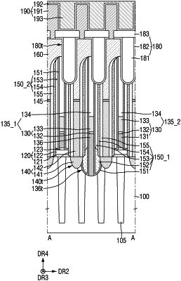
1. A semiconductor device comprising:
a substrate having a trench and a contact recess;
a conductive pattern in the trench and having a width less than a width of the trench;
a spacer structure on a side surface of the conductive pattern; and
a buried contact including a first portion spaced apart from the conductive pattern by the spacer structure and filling the contact recess, and a second portion on the first portion, the second portion having a pillar shape having a width less than a width of a top surface of the first portion,
wherein the contact recess has a curved profile,
the spacer structure includes a first spacer at an outermost side, the first spacer on the first portion of the buried contact, extending along the second portion of the buried contact, contacting the buried contact, and contacting the top surface of the first portion, a second spacer extending on the first spacer along the first spacer, and a third spacer extending along the side surface of the conductive pattern and the trench and spaced apart from the first spacer by the second spacer, and
the first spacer includes silicon oxide, and the second spacer includes silicon nitride.
|