| CPC H01L 29/6656 (2013.01) [H01L 29/0673 (2013.01); H01L 29/1033 (2013.01); H01L 29/1079 (2013.01); H01L 29/66545 (2013.01); H01L 29/66553 (2013.01); B82Y 10/00 (2013.01)] | 20 Claims |
|
1. A semiconductor device comprising:
first and second active patterns each extending in a first direction and spaced apart from each other in a second direction that is perpendicular to the first direction;
a field insulating layer disposed between the first active pattern and the second active pattern;
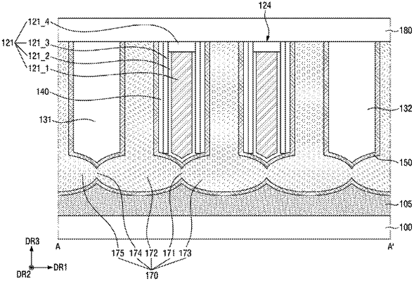
a first gate structure disposed on the first active pattern and extending in the second. direction;
an interlayer insulating layer disposed between the first gate structure and the field insulating layer, the interlayer insulating layer including a first part disposed below the first gate structure; and
a spacer disposed between the first gate structure and the first part of the interlayer insulating layer, wherein an upper surface of the spacer has a height that is greater than a height of lowermost surface of the first gate structure.
|