| CPC H01L 29/66462 (2013.01) [H01L 21/28264 (2013.01); H01L 21/28581 (2013.01); H01L 29/2003 (2013.01); H01L 29/205 (2013.01); H01L 29/475 (2013.01); H01L 29/66431 (2013.01); H01L 29/7786 (2013.01); C23C 14/0021 (2013.01); C23C 14/0641 (2013.01); C23C 14/0676 (2013.01); C23C 14/30 (2013.01); H01L 29/41766 (2013.01)] | 20 Claims |

|
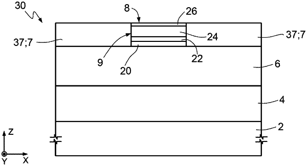
1. A high electron mobility transistor (HEMT) device of a normally-on type, comprising:
a semiconductor heterostructure;
a dielectric layer extending over the semiconductor heterostructure and including a trench including sidewalls; and
a gate electrode extending through the trench in the dielectric layer, wherein the gate electrode is a stack, which includes:
a protection layer, made of a metal nitride with stuffed grain boundaries, extending over the semiconductor heterostructure;
a first metal layer extending over the protection layer and completely separated from the semiconductor heterostructure by said protection layer;
a second metal layer below the protection layer in contact with the semiconductor heterostructure and of a material that is able to form a Schottky junction with the semiconductor heterostructure; and
a cap layer on the first metal layer, wherein the protection layer, the first metal laver, the second metal layer, and the cap layer are each in contact with the dielectric layer at the sidewalls of the trench.
|