| CPC H01L 29/511 (2013.01) [H01L 29/0669 (2013.01); H01L 29/1033 (2013.01)] | 15 Claims |
|
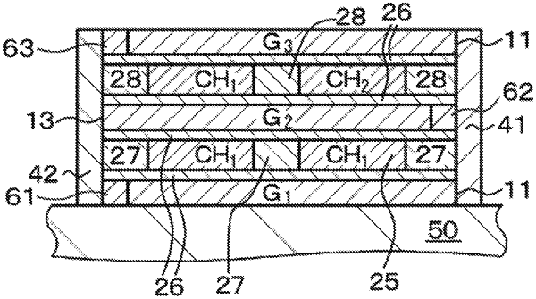
1. A semiconductor device, comprising:
a stacked structure having a channel formation region layers and gate electrode layers alternately arranged on top of each other on a base,
wherein a lowermost layer of the stacked structure is formed with a 1st layer of the gate electrode layers,
wherein an uppermost layer of the stacked structure is formed with an Nth (where N≥3) layer of the gate electrode layers, and
wherein each channel formation region layer includes at least one channel structure portion and each channel structure portion includes extensions provided on each end of the at least one channel structure portion.
|