| CPC H01L 29/42392 (2013.01) [H01L 21/308 (2013.01); H01L 21/3065 (2013.01); H01L 21/30604 (2013.01); H01L 21/31116 (2013.01); H01L 21/31144 (2013.01); H01L 21/8221 (2013.01); H01L 21/823878 (2013.01); H01L 21/84 (2013.01); H01L 27/0688 (2013.01); H01L 29/66545 (2013.01); H01L 29/66742 (2013.01); H01L 29/7848 (2013.01); H01L 29/78603 (2013.01); H01L 29/78696 (2013.01); H01L 29/165 (2013.01)] | 9 Claims |
|
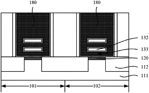
1. A semiconductor structure, comprising:
a semiconductor substrate;
a plurality of fins protruding from the semiconductor substrate, a first fin of the plurality of fins being formed on a PMOS region, and a second fin of the plurality of fins being formed on an NMOS region, the second fin being adjacent to the first fin;
an isolation layer formed on the first fin and the second fin and with a bandgap greater than a bandgap of the fins, the isolation layer being made of a material including at least one of GaN or AlGaN;
a first channel layer formed over each of the first fin and the second fin, the first channel layer being isolated from the isolation layer;
a dummy gate structure formed across the first fin and the second fin and cover the top surfaces and sidewall surfaces of the first channel layer;
a first gate opening and a second gate opening formed in the dummy gate structure on the PMOS region and the NMOS region, respectively, a portion of the dummy gate structure being located between the first gate opening and the second gate opening;
a gate dielectric layer covering bottom surfaces and sidewall surfaces of the first gate opening and the second gate opening, and to cover top surfaces, bottom surfaces, and sidewall surfaces of the first channel layer in the first gate opening and the second gate opening, a gap being located between the gate dielectric layer under the first channel layer and the gate dielectric layer on the bottom surface of each of the first gate opening and the second gate opening; and
an all-around gate structure formed in each of the first gate opening and the second gate opening to fill the gap, wherein the all-around gate structure covers the gate dielectric layer on the top surfaces, the bottom surfaces, and the sidewall surfaces of the first channel layer in the first and second gate openings.
|