US 11,728,398 B2
Device and method for managing electromagnetic radiation
Michael Shur, Vienna, VA (US); and David J. Meyer, Fairfax, VA (US)
Assigned to The Government of the United States of America, as represented by the Secretary of the Navy, Washington, DC (US)
Filed by The Government of the United States of America, as represented by the Secretary of the Navy, Arlington, VA (US)
Filed on Jul. 14, 2020, as Appl. No. 16/928,243.
Claims priority of provisional application 62/890,627, filed on Aug. 23, 2019.
Prior Publication US 2021/0057534 A1, Feb. 25, 2021
Int. Cl. H01L 27/146 (2006.01); H01L 29/423 (2006.01); H01L 29/788 (2006.01); H01L 29/66 (2006.01); H01L 23/552 (2006.01)
CPC H01L 29/42328 (2013.01) [H01L 23/552 (2013.01); H01L 27/14649 (2013.01); H01L 27/14658 (2013.01); H01L 27/14689 (2013.01); H01L 29/66825 (2013.01); H01L 29/788 (2013.01)] 20 Claims
OG exemplary drawing
 
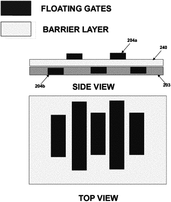
1. A semiconductor device having a plurality of separated floating gates directly embedded within a conducting channel within the semiconductor device;
wherein each one of the plurality of separated floating gates is spaced-apart from another one of the plurality of separated floating gates within the conducting channel;
wherein each of the plurality of separated floating gates has a size smaller than a mean free path of electrons in the semiconductor device.