| CPC H01L 29/24 (2013.01) [H01L 29/0692 (2013.01); H01L 29/1037 (2013.01); H01L 29/42384 (2013.01); H01L 29/4908 (2013.01); H01L 29/7869 (2013.01); H01L 29/78648 (2013.01); H01L 29/78696 (2013.01)] | 18 Claims |
|
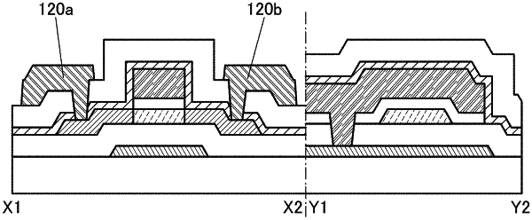
1. A semiconductor device comprising:
a substrate;
an oxide semiconductor layer over the substrate, the oxide semiconductor layer comprising:
a plurality of first regions; and
a plurality of second regions;
a gate insulating layer over the oxide semiconductor layer;
a gate electrode over the gate insulating layer; and
a source electrode and a drain electrode over the gate insulating layer,
wherein the oxide semiconductor layer comprises In, Zn, and element M,
wherein element M is one of Ga, Al, Hf, Y and Sn,
wherein each of In concentrations in the plurality of first regions is higher than each of In concentrations in the plurality of second regions,
wherein the plurality of first regions comprise two first regions arranged in a parallel direction to a top surface of the substrate in a cross-sectional image of the semiconductor device,
wherein the plurality of second regions comprise two second regions arranged in a parallel direction to the top surface of the substrate in the cross-sectional image of the semiconductor device,
wherein one of the plurality of first regions is interposed between the two second regions,
wherein the one of the plurality of first regions has a diameter greater than or equal to 0.5 nm and less than or equal to 10 nm in the cross-sectional image,
wherein one of the plurality of second regions is interposed between the two first regions, and
wherein the one of the plurality of second regions has a diameter greater than or equal to 0.5 nm and less than or equal to 10 nm in the cross-sectional image.
|