| CPC H01L 29/24 (2013.01) [H01L 29/1606 (2013.01); H01L 29/267 (2013.01); H01L 29/66545 (2013.01); H01L 29/66636 (2013.01); H01L 29/66795 (2013.01); H01L 29/7851 (2013.01)] | 20 Claims |
|
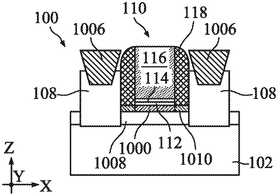
1. A method, comprising:
providing a workpiece having a semiconductor structure;
depositing a two-dimensional (2D) material layer over the semiconductor structure;
forming a dielectric feature inserted between the 2D material layer and the semiconductor structure;
forming a source feature and a drain feature electrically connected to the semiconductor structure and the 2D material layer, wherein the source feature and drain feature include a semiconductor material; and
forming a gate structure over the two-dimensional material layer and interposed between the source feature and the drain feature, wherein the gate structure, the source feature, the drain feature, the semiconductor structure and the 2D material layer are configured to form a field-effect transistor, and wherein the semiconductor structure and the 2D material layer function, respectively, as a first channel and a second channel between the source feature and the drain feature.
|