| CPC H01L 29/161 (2013.01) [H01L 29/1041 (2013.01); H01L 29/7848 (2013.01)] | 20 Claims |
|
1. A method for manufacturing a semiconductor device, the method comprising:
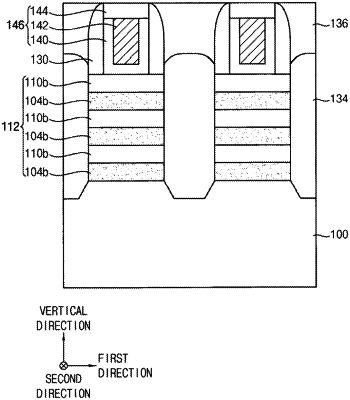
alternately and repeatedly stacking a silicon germanium layer and a silicon layer on a substrate in a vertical direction perpendicular to a surface of the substrate to form a stacked structure;
forming silicon-rich silicon germanium layers from the silicon germanium layer by ion implanting silicon on the stacked structure;
patterning the stacked structure to form a preliminary active structure extending in a first direction parallel to the surface of the substrate;
patterning the preliminary active structure to form an active structure including silicon germanium patterns and silicon patterns that are alternately and repeatedly stacked in the vertical direction;
forming a semiconductor layer formed on both sidewalls of the active structure and serving as a source/drain region; and,
forming a gate structure on a surface of the active structure and on the substrate, the gate structure extending in a second direction parallel to the substrate surface and perpendicular to the first direction.
|