| CPC H01L 29/1608 (2013.01) [H01L 29/0603 (2013.01); H01L 29/0696 (2013.01); H01L 29/1095 (2013.01); H01L 29/7802 (2013.01)] | 2 Claims |
|
1. A semiconductor device comprising:
a silicon carbide layer having a first plane and a second plane,
the silicon carbide layer including
an element region and
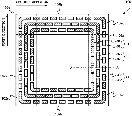
a termination region surrounding the element region, the termination region having first straight-line portions extending in a first direction, second straight-line portions extending in a second direction intersecting the first direction, and corner portions between the first straight-line portions and the second straight-line portions,
the termination region including
a first silicon carbide region of first-conductivity-type, and
a second silicon carbide region of second-conductivity-type provided between the first silicon carbide region and the first plane, the second silicon carbide region surrounding the element region, the second silicon carbide region having a dot-line shape configured with first dot portions and first space portions between the first dot portions, an occupation ratio of the first dot portions of the corner portions being larger than an occupation ratio of the first dot portions of the first straight-line portions;
a first electrode provided on a side of the first plane of the silicon carbide layer; and
a second electrode provided on a side of the second plane of the silicon carbide layer.
|