| CPC H01L 29/1054 (2013.01) [H01L 21/265 (2013.01); H01L 29/7606 (2013.01)] | 10 Claims |
|
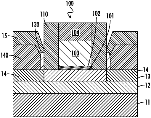
1. A method of fabricating a P-type Field Effect Transistor (PFET) device using fully depleted silicon on insulator (FDSOI) technology, comprising:
forming a gate on a workpiece, the workpiece comprising a bulk region, a buried oxide layer and a channel layer; wherein the gate comprises a Hi-K/SiO2 bi-layer, a work function metal, a polysilicon layer and a cap layer;
implanting germanium ions into the channel layer in regions that are not beneath the gate to form SiGe stressors in the channel layer so as to increase axial stress in the channel layer, wherein a concentration of germanium in the SiGe stressors after implanting is greater than 40%;
performing a thermal treatment to recrystallize the SiGe stressors after the implanting;
growing raised source and drain regions on the SiGe stressors on both sides of the gate;
forming spacers on both sides of the gate before the implanting;
depositing an oxide layer on the workpiece after the spacers are formed and prior to the thermal treatment; and
removing at least a portion of the oxide layer after the thermal treatment and prior to growing the raised source and drain regions.
|