| CPC H01L 29/0649 (2013.01) [H01L 21/7682 (2013.01); H01L 29/41775 (2013.01); H01L 29/4991 (2013.01); H01L 29/6653 (2013.01); H01L 29/66575 (2013.01); H01L 21/764 (2013.01); H01L 29/78 (2013.01)] | 6 Claims |
|
1. A semiconductor device, comprising:
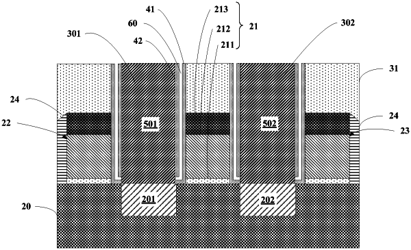
a substrate, comprising a source and a drain;
a gate structure disposed on the substrate, wherein the source and the drain are respectively located on two sides of the gate structure;
a first inter-layer dielectric layer covering the gate structure;
a source contact hole running through the first inter-layer dielectric layer and exposing the source and a drain contact hole running through the first inter-layer dielectric layer and exposing the drain;
a source contact member connected to the source in the source contact hole and a drain contact member connected to the drain in the drain contact hole;
an air gap between the gate structure and the source contact member or between the gate structure and the drain contact member, wherein side walls of the air gap are a side wall of the gate structure and a side wall of the source contact member or a side wall of the gate structure and a side wall of the drain contact member; and
a second inter-layer dielectric layer on the first inter-layer dielectric layer, the source contact member, and the drain contact member, wherein the second inter-layer dielectric layer covers the air gap, a top end of the air gap is level with a top surface of the first inter-layer dielectric layer and a bottom surface of the second inter-layer dielectric layer.
|