| CPC H01L 28/56 (2013.01) [H01L 21/02181 (2013.01); H01L 21/02189 (2013.01); H01L 21/02192 (2013.01); H01L 21/02197 (2013.01); H01L 21/28247 (2013.01); H10B 53/30 (2023.02); H10B 12/00 (2023.02)] | 18 Claims |
|
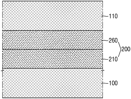
1. A semiconductor device comprising:
first and second electrodes apart from each other; and
a capacitor dielectric film between the first electrode and the second electrode and including a first dielectric film and a second dielectric film, the first dielectric film being between the second dielectric film and the first electrode,
wherein each of the first dielectric film and the second dielectric film includes a metal oxide film,
a metal contained in the metal oxide film is contained in a transition metal of group 4 (IV B) of a periodic table,
the first dielectric film has an orthorhombic crystal system,
the metal oxide film included in the second dielectric film is a paraelectric material, and
the second dielectric film has a monoclinic crystal system.
|