| CPC H01L 27/156 (2013.01) [H01L 24/08 (2013.01); H01L 24/89 (2013.01); H01L 25/18 (2013.01); H01L 27/124 (2013.01); H01L 27/1248 (2013.01); H01L 33/0075 (2013.01); H01L 33/32 (2013.01); H01L 33/382 (2013.01); H01L 33/46 (2013.01); H01L 33/502 (2013.01); H01L 33/505 (2013.01); H01L 33/62 (2013.01); H01L 2224/08146 (2013.01); H01L 2224/08147 (2013.01); H01L 2224/80001 (2013.01); H01L 2933/0016 (2013.01); H01L 2933/0025 (2013.01); H01L 2933/0041 (2013.01); H01L 2933/0066 (2013.01)] | 20 Claims |
|
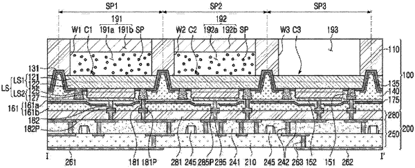
1. A method of fabricating an LED module, comprising:
forming a semiconductor structure having a first conductivity-type semiconductor layer on a substrate;
dividing the semiconductor structure into a plurality of lower light emitting structures by forming an isolation region to which a surface of the substrate is exposed;
forming a protective insulating film on upper and side surfaces of the plurality of lower light emitting structures and the exposed surface of the substrate;
forming a light blocking film on a portion of the protective insulating film located in the isolation region;
forming a gap-fill insulating film on the protective insulating film to fill the isolation region;
partially removing the gap-fill insulating film and the protective insulating film to expose a portion of an upper surface of each of the plurality of lower light emitting structures;
forming an upper light emitting structure having an active layer and a second conductivity-type semiconductor layer sequentially disposed on the exposed portion of the upper surface of each of the plurality of lower light emitting structures; and
forming a first electrode and a second electrode connected to the first conductivity-type semiconductor layer and the second conductivity-type semiconductor layer, respectively, the first electrode penetrating through the gap-fill insulating film and the protective insulating film.
|