| CPC H01L 27/156 (2013.01) [G09G 3/32 (2013.01); H01L 33/502 (2013.01); H01L 33/60 (2013.01); H01L 33/62 (2013.01)] | 19 Claims |
|
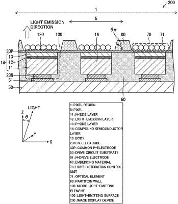
1. An image display device comprising:
micro light-emitting elements;
a drive circuit substrate including a drive circuit that supplies currents to the micro light-emitting elements to emit light, wherein the micro light-emitting elements are arranged in an array shape on the drive circuit substrate;
light-distribution control units that increase forward light emission of the micro light-emitting elements, each of the light-distribution control units being disposed on a light-emitting surface of a corresponding one of the micro light-emitting elements; and
a partition wall, disposed around the light-distribution control units, that does not transmit the light emitted by the micro light-emitting elements, wherein the partition wall forms a portion of a wire that supplies the currents to the micro light-emitting elements.
|