US 11,728,366 B2
Extra doped region for back-side deep trench isolation
Chun-Yuan Chen, Tainan (TW); Ching-Chun Wang, Tainan (TW); Dun-Nian Yaung, Taipei (TW); Hsiao-Hui Tseng, Tainan (TW); Jhy-Jyi Sze, Hsin-Chu (TW); Shyh-Fann Ting, Tainan (TW); Tzu-Jui Wang, Fengshan (TW); Yen-Ting Chiang, Tainan (TW); Yu-Jen Wang, Kaohsiung (TW); and Yuichiro Yamashita, Hsinchu (TW)
Assigned to Taiwan Semiconductor Manufacturing Company, Ltd., Hsinchu (TW)
Filed by Taiwan Semiconductor Manufacturing Company, Ltd., Hsin-Chu (TW)
Filed on Nov. 5, 2021, as Appl. No. 17/519,784.
Application 16/352,108 is a division of application No. 15/919,784, filed on Mar. 13, 2018, granted, now 10,276,618, issued on Apr. 30, 2019.
Application 17/519,784 is a continuation of application No. 16/674,216, filed on Nov. 5, 2019, granted, now 11,227,889.
Application 16/674,216 is a continuation of application No. 16/352,108, filed on Mar. 13, 2019, granted, now 10,510,789, issued on Dec. 17, 2019.
Application 15/919,784 is a continuation of application No. 14/923,635, filed on Oct. 27, 2015, granted, now 9,954,022, issued on Apr. 24, 2018.
Prior Publication US 2022/0059583 A1, Feb. 24, 2022
Int. Cl. H01L 27/146 (2006.01)
CPC H01L 27/1463 (2013.01) [H01L 27/1464 (2013.01); H01L 27/14643 (2013.01); H01L 27/14689 (2013.01); H01L 27/14609 (2013.01); H01L 27/14621 (2013.01); H01L 27/14627 (2013.01)] 20 Claims
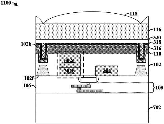
OG exemplary drawing
 
1. An integrated chip, comprising:
an image sensor disposed within a semiconductor substrate, wherein the semiconductor substrate comprises sidewalls that form one or more trenches extending from a first surface of the semiconductor substrate to within the semiconductor substrate;
one or more isolation structures arranged within the one or more trenches, wherein the semiconductor substrate covers an entire bottom surface of the one or more isolation structures;
a doped region arranged within the semiconductor substrate vertically between the first surface of the semiconductor substrate and a top of the image sensor facing the first surface of the semiconductor substrate; and
wherein the doped region has a higher concentration of a first dopant type than an abutting part of the semiconductor substrate that extends along opposing sides of the image sensor.