| CPC H01L 27/14627 (2013.01) [H01L 27/14621 (2013.01)] | 12 Claims |
|
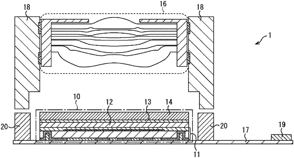
1. A solid-state imaging device, comprising:
a transparent protective substrate;
a solid-state imaging element;
a bonding resin layer; and
a high refractive index layer in a light incident direction, wherein
a refractive index of the high refractive index layer is higher than a refractive index of one of the transparent protective substrate or a surface layer of an imaging surface of the solid-state imaging element,
a refractive index of the bonding resin layer is lower than the refractive index of the high refractive index layer,
the high refractive index layer is between the transparent protective substrate and the solid-state imaging element, and
the high refractive index layer is between the solid-state imaging element and the bonding resin layer.
|