| CPC H01L 27/14623 (2013.01) [H01L 27/14621 (2013.01); H01L 27/14627 (2013.01); H01L 27/14645 (2013.01); H01L 27/14685 (2013.01); H01L 27/14689 (2013.01)] | 12 Claims |
|
1. An imaging device, comprising:
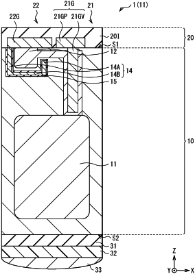
a photoelectric converter configured to generate a signal charge;
a charge holding section on a side of the photoelectric converter that is opposite to a light entrance side of the photoelectric converter, wherein the charge holding section is configured to hold the generated signal charge;
a light shielding section that includes a first light shielding surface between the charge holding section and the photoelectric converter; and
a vertical electrode section, wherein
the charge holding section has a specific surface parallel to the vertical electrode section,
the specific surface of the charge holding section and the vertical electrode section are parallel to a first direction, and
in a second direction perpendicular to the first direction, the first light shielding surface is between the vertical electrode section and the specific surface of the charge holding section.
|