| CPC H01L 27/14621 (2013.01) [H01L 27/1462 (2013.01); H01L 27/14618 (2013.01); H01L 27/14623 (2013.01); H01L 27/14627 (2013.01); H01L 27/14632 (2013.01); H01L 27/14685 (2013.01); H01L 27/14687 (2013.01)] | 18 Claims |
|
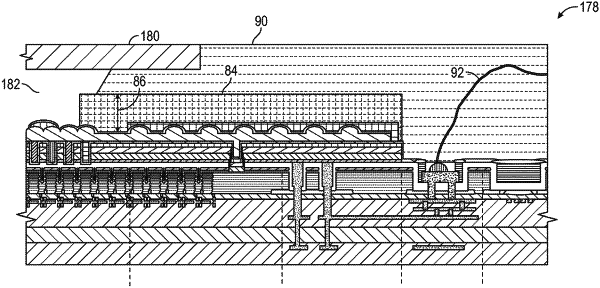
1. A method of forming an image sensor package comprising:
forming an encapsulation layer around a perimeter of one or more lenses, the encapsulation layer comprising a largest planar surface substantially parallel with a largest planar surface of a lens layer comprising the one or more lenses;
forming a temporary protection layer over the one or more lenses, the temporary protection layer formed through an opening in the encapsulation layer;
depositing a mold compound over the encapsulation layer, the mold compound comprising a largest planar surface substantially parallel with the largest planar surface of the lens layer; and
removing the temporary protection layer over the one or more lenses;
wherein a dam structure separates the encapsulation layer from the temporary protection layer.
|