| CPC H01L 27/14616 (2013.01) [H01L 27/1463 (2013.01); H04N 25/75 (2023.01); H04N 25/76 (2023.01)] | 12 Claims |
|
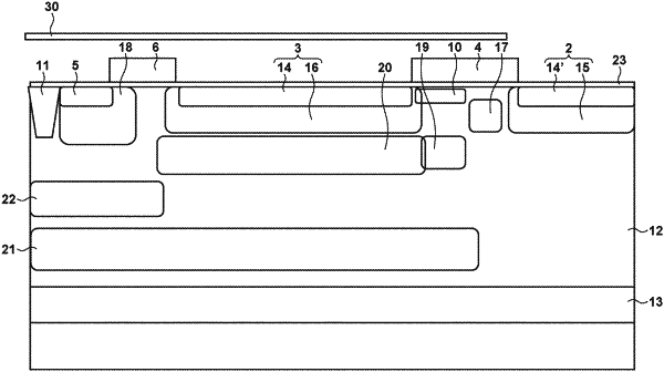
1. A photoelectric conversion apparatus comprising:
a semiconductor layer including a first surface and a second surface;
a first semiconductor region of a first conductivity type arranged in the semiconductor layer and configured to accumulate a signal charge generated by incident light;
a second semiconductor region of the first conductivity type arranged in the semiconductor layer;
a first transfer electrode arranged on the first surface and configured to form, in the semiconductor layer, a channel for transferring the signal charge accumulated in the first semiconductor region to the second semiconductor region;
a third semiconductor region of a second conductivity type arranged between the second semiconductor region and the second surface; and
a fourth semiconductor region of the second conductivity type arranged between the third semiconductor region and the second surface;
wherein the third semiconductor region at least partially overlaps the second semiconductor region in orthographic projection to the first surface,
the third semiconductor region at least partially overlaps the fourth semiconductor region in orthographic projection to the first surface, and
an effective value of an impurity concentration of an intermediate semiconductor region of the second conductivity type between the third semiconductor region and the fourth semiconductor region is not less than 2×1013 cm−3 and not more than 1×1015 cm−3, and a width of the intermediate semiconductor region in a normal direction with respect to the first surface is not less than 0.13 μm and not more than 0.8 μm.
|