| CPC H01L 27/14609 (2013.01) [G02B 7/34 (2013.01); G02B 7/38 (2013.01); G02B 13/0085 (2013.01); H01L 27/14607 (2013.01); H01L 27/14625 (2013.01); H01L 27/14627 (2013.01); H01L 27/14645 (2013.01); H01L 27/14665 (2013.01); H04N 23/672 (2023.01); H04N 23/673 (2023.01); H04N 25/704 (2023.01); G03B 13/36 (2013.01)] | 20 Claims |
|
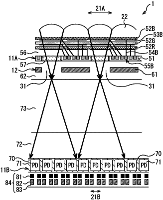
1. A solid-state imaging device comprising:
an organic photoelectric conversion film, wherein the organic photoelectric conversion film comprises two or more laminated photoelectric conversion layers, wherein each photoelectric conversion layer includes a photoelectric converter and a charge detector;
a copper-to-copper (“Cu—Cu”) metal coupling;
a lower-side substrate;
one or more photodiodes formed on the lower-side substrate;
an intermediate layer between the organic photoelectric conversion film and the one or more photodiodes; and
a multi-layer wiring layer bonded to the lower-side substrate via the Cu—Cu metal coupling.
|