US 11,728,355 B2
Imaging device and electronic device
Takayuki Ikeda, Kanagawa (JP); Yoshiyuki Kurokawa, Kanagawa (JP); Shintaro Harada, Kanagawa (JP); Hidetomo Kobayashi, Kanagawa (JP); Roh Yamamoto, Toyama (JP); Kiyotaka Kimura, Kanagawa (JP); Takashi Nakagawa, Kanagawa (JP); and Yusuke Negoro, Kanagawa (JP)
Assigned to Semiconductor Energy Laboratory Co., Ltd., Atsugi (JP)
Filed by SEMICONDUCTOR ENERGY LABORATORY CO., LTD., Atsugi (JP)
Filed on Aug. 17, 2021, as Appl. No. 17/403,911.
Application 17/403,911 is a continuation of application No. 16/615,156, granted, now 11,101,302, previously published as PCT/IB2018/053400, filed on May 16, 2018.
Claims priority of application No. 2017-104338 (JP), filed on May 26, 2017; and application No. 2018-040915 (JP), filed on Mar. 7, 2018.
Prior Publication US 2021/0384239 A1, Dec. 9, 2021
This patent is subject to a terminal disclaimer.
Int. Cl. H01L 27/146 (2006.01); H01L 27/12 (2006.01); H01L 29/786 (2006.01); H04N 25/40 (2023.01); H04N 25/77 (2023.01); H04N 25/766 (2023.01)
CPC H01L 27/14605 (2013.01) [H01L 27/1225 (2013.01); H01L 27/14612 (2013.01); H01L 27/14643 (2013.01); H01L 29/7869 (2013.01); H04N 25/40 (2023.01); H04N 25/766 (2023.01); H04N 25/77 (2023.01)] 4 Claims
OG exemplary drawing
 
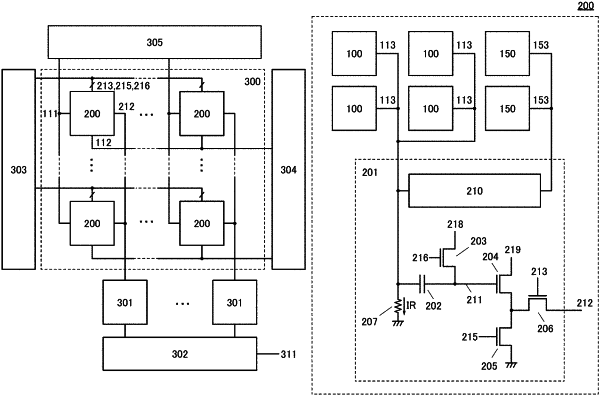
1. An imaging device comprising:
a pixel block comprising a pixel and a second circuit; and
a first circuit,
wherein the pixel is configured to obtain a first signal by photoelectric conversion,
wherein the second circuit is configured to generate a second signal on the basis of a sum of the first signals, and
wherein the first circuit is configured to generate a third signal by binarizing the second signal.