| CPC H01L 27/14603 (2013.01) [G09G 3/3648 (2013.01); H01L 27/14612 (2013.01); H01L 27/14616 (2013.01); H01L 27/14625 (2013.01); H01L 27/14636 (2013.01); H01L 27/14641 (2013.01); H01L 27/14643 (2013.01); H01L 29/7869 (2013.01); G09G 2354/00 (2013.01)] | 9 Claims |
|
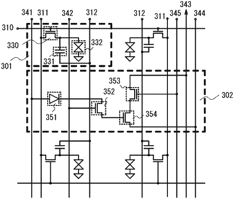
1. An electronic device comprising:
a photodiode;
a first transistor;
a second transistor; and
a third transistor,
wherein a first electrode of the photodiode is electrically connected to a first wire,
wherein a second electrode of the photodiode is electrically connected to one of a source and a drain of the first transistor,
wherein the other of the source and the drain of the first transistor is electrically connected to a gate of the second transistor,
wherein one of a source and a drain of the second transistor is electrically connected to a second wire,
wherein the other of the source and the drain of the second transistor is electrically connected to one of a source and a drain of the third transistor,
wherein the other of the source and the drain of the third transistor is electrically connected to a third wire,
wherein a gate of the first transistor is electrically connected to a fourth wire,
wherein a gate of the third transistor is electrically connected to a fifth wire,
wherein the first wire is electrically connected to a sixth wire,
wherein the first wire and the sixth wire cross each other, and
wherein the first wire and the fifth wire cross each other.
|