| CPC H01L 27/142 (2013.01) [H01L 27/14685 (2013.01); H01L 31/0463 (2014.12); H01L 31/18 (2013.01); H10K 30/211 (2023.02); Y02E 10/549 (2013.01)] | 24 Claims |
|
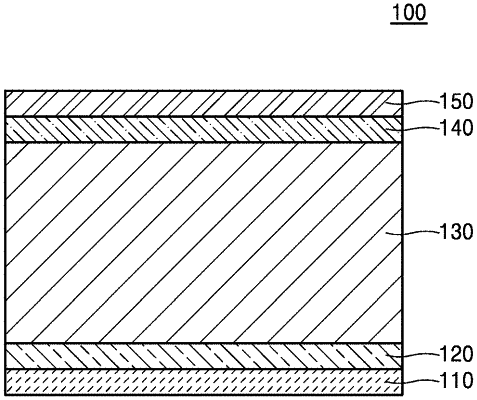
1. A photoelectric conversion device comprising:
a first conductive layer;
a second conductive layer;
a photoelectric conversion layer between the first conductive layer and the second conductive layer;
an electron blocking layer between the photoelectric conversion layer and the first conductive layer; and
a hole blocking layer between the photoelectric conversion layer and the second conductive layer,
wherein the electron blocking layer comprises a first perovskite compound represented by Formula 1, and the hole blocking layer comprises a second perovskite compound represented by Formula 2,
[A1][B1][X1(3-n)Y1n] Formula 1
wherein, in Formula 1,
A1 comprises a monovalent organic cation, a monovalent inorganic cation, or a combination thereof,
B1 comprises a divalent inorganic cation,
X1 and Y1 each independently comprises a monovalent anion, and
n is a real number satisfying 0≤n≤3, and
[A2][B2][X2(3-m)Y2m] Formula 2
wherein, in Formula 2,
A2 comprises a monovalent organic cation, a monovalent inorganic cation, or a combination thereof,
B2 comprises a divalent inorganic cation,
X2 and Y2 each independently comprises a monovalent anion, and
m is a real number satisfying 0≤m≤3,
wherein the electron blocking layer further comprises a polar polymer, the hole blocking layer further comprises a polar polymer, or a combination thereof, and
wherein the polar polymer comprises polyamic acid, polyimide, polyvinyl alcohol, polyacrylic acid, polyhydroxyethyl methacrylate, polymethyl methacrylate, polyacrylate, polyacrylonitrile, or a combination thereof.
|