| CPC H01L 27/124 (2013.01) [G09G 3/20 (2013.01); G09G 2310/0272 (2013.01)] | 19 Claims |
|
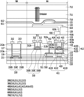
1. A display device comprising:
a substrate comprising a display area and a non-display area;
a first thin-film transistor located in the non-display area; and
a second thin-film transistor and a third thin-film transistor located in the display area,
wherein the first thin-film transistor comprises:
a first semiconductor pattern comprising a first poly silicon;
a first gate electrode overlapping the first semiconductor pattern; and
a first source electrode and a first drain electrode connected to the first semiconductor pattern,
wherein the second thin-film transistor comprises:
a second semiconductor pattern and a third semiconductor pattern comprising a first oxide semiconductor;
a second gate electrode overlapping the second semiconductor pattern;
a third gate electrode overlapping the third semiconductor pattern;
a second source electrode and a second drain electrode connected to the second semiconductor pattern and the third semiconductor pattern through a contact hole;
a first insulation film provided between the second semiconductor pattern and the second gate electrode; and
a second insulation film provided between the second semiconductor pattern and the first insulation film, wherein the first insulation film has a higher hydrogen particle content than the second insulation film, and
wherein the third thin-film transistor comprises:
a fourth semiconductor pattern comprising a first oxide semiconductor;
a fourth gate electrode overlapping the fourth semiconductor pattern; and
a third source electrode and a third drain electrode connected to the fourth semiconductor pattern.
|