| CPC H01L 27/1225 (2013.01) [G02F 1/13454 (2013.01); H01L 27/124 (2013.01); H01L 27/1285 (2013.01); H01L 29/045 (2013.01); H01L 29/66742 (2013.01); H01L 29/66969 (2013.01); H01L 29/7869 (2013.01); G02F 1/1368 (2013.01); G02F 1/13452 (2013.01); G02F 1/133345 (2013.01); G02F 1/134309 (2013.01); G02F 1/136286 (2013.01); G02F 2201/123 (2013.01); G09G 3/3266 (2013.01); G09G 3/3275 (2013.01); G09G 3/3677 (2013.01); G09G 3/3688 (2013.01); G09G 2300/0426 (2013.01); G09G 2310/0286 (2013.01); G09G 2310/08 (2013.01); G09G 2330/023 (2013.01)] | 12 Claims |
|
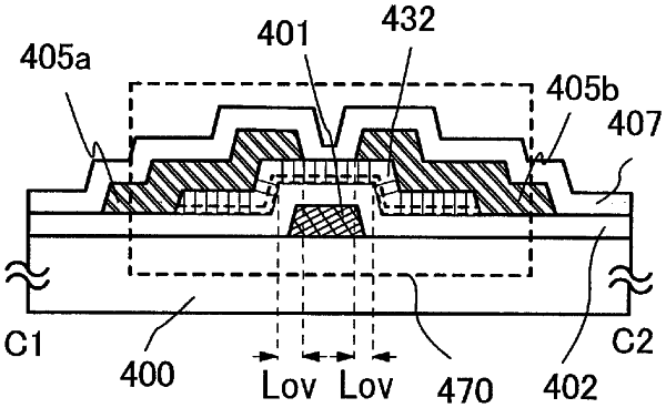
1. A semiconductor device comprising:
a substrate comprising a top surface;
a gate electrode layer over the substrate, and comprising a top surface and a side surface, the side surface having an inclination with respect to the top surface of the substrate;
a first oxide semiconductor layer over the substrate with the gate electrode layer interposed therebetween;
a second oxide semiconductor layer over the first oxide semiconductor layer; and
a gate insulating layer between the gate electrode layer and the first oxide semiconductor layer,
wherein the second oxide semiconductor layer comprises a first region overlapping with the top surface of the gate electrode layer and a second region inclined in response to the inclination of the side surface of the gate electrode layer,
wherein a first crystal in the first region of the second oxide semiconductor layer has a c-axis alignment along a thickness direction of the first region of the second oxide semiconductor layer,
wherein a second crystal in the second region of the second oxide semiconductor layer has a c-axis alignment along a thickness direction of the second region of the second oxide semiconductor layer, and
wherein a direction of a c-axis of the first crystal is different from a direction of a c-axis of the second crystal.
|