| CPC H01L 27/1203 (2013.01) [H01L 21/76224 (2013.01); H01L 27/0203 (2013.01); H01L 27/02 (2013.01); H01L 29/78 (2013.01)] | 8 Claims |
|
1. A method of manufacturing an integrated circuit device, the method comprising:
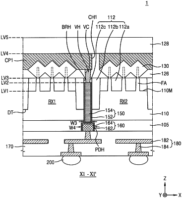
preparing a semiconductor-on-insulator (SOI) substrate, on which a base substrate layer, an embedded insulation layer, and a semiconductor layer are sequentially stacked;
forming a deep trench that defines at least two element regions, by partially removing the semiconductor layer;
forming a preliminary separation insulation layer to fill the deep trench;
forming a buried rail hole that penetrates through the preliminary separation insulation layer and the semiconductor layer, a buried rail partially filled in a lower portion of the buried rail hole, and a preliminary cover insulation layer filled in an upper portion of the buried rail hole;
exposing the embedded insulation layer by removing the base substrate layer; and
forming a power delivery structure in the embedded insulation layer, the power delivery structure being in contact with the buried rail.
|