| CPC H01L 27/0924 (2013.01) [H01L 21/823807 (2013.01); H01L 21/823814 (2013.01); H01L 21/823821 (2013.01); H01L 21/823878 (2013.01); H01L 27/092 (2013.01); H01L 29/045 (2013.01); H01L 29/0665 (2013.01); H01L 29/165 (2013.01); H01L 29/42392 (2013.01); H01L 29/6656 (2013.01); H01L 29/66545 (2013.01); H01L 29/78696 (2013.01)] | 20 Claims |
|
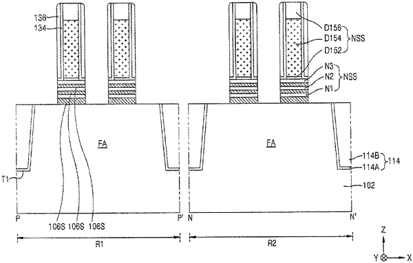
1. A semiconductor device, comprising:
a substrate;
a fin protruding from the substrate;
a plurality of nanosheets disposed on the fin;
a gate disposed on the fin, the gate including a main gate portion on the plurality of nanosheets, and a plurality of sub-gate portions between the plurality of nanosheets and the fin;
a source/drain disposed on the fin, an outer edge region of an upper surface of the source/drain being higher in vertical position relative to an inner region thereof; and
a plurality of insulating spacers disposed on sidewalls of the plurality of sub-gate portions,
wherein:
the plurality of sub-gate portions include a first sub-gate portion, and a second sub-gate portion disposed above the first sub-gate portion, and
a volume of the first sub-gate portion is greater than a volume of the second sub-gate portion.
|