| CPC H01L 27/0922 (2013.01) [H01L 21/02529 (2013.01); H01L 21/02532 (2013.01); H01L 21/02603 (2013.01); H01L 21/187 (2013.01); H01L 21/28088 (2013.01); H01L 21/82345 (2013.01); H01L 21/823412 (2013.01); H01L 21/823418 (2013.01); H01L 21/823475 (2013.01); H01L 29/0673 (2013.01); H01L 29/161 (2013.01); H01L 29/1608 (2013.01); H01L 29/41733 (2013.01); H01L 29/42392 (2013.01); H01L 29/4908 (2013.01); H01L 29/4966 (2013.01); H01L 29/66545 (2013.01); H01L 29/66742 (2013.01); H01L 29/78618 (2013.01); H01L 29/78684 (2013.01); H01L 29/78696 (2013.01)] | 20 Claims |
|
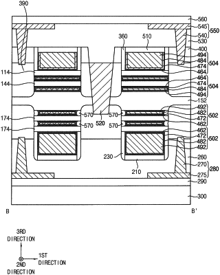
1. A method of manufacturing a semiconductor device, the method comprising:
forming a line stack structure on a first substrate, the line stack structure including a first line, a division pattern and a second line sequentially stacked in a vertical direction perpendicular to an upper surface of the first substrate, the first line including a first sacrificial line and a first semiconductor line alternately stacked in the vertical direction, and the second line including a second sacrificial line and a second semiconductor line alternately stacked in the vertical direction;
forming a first dummy gate structure on the first substrate to partially cover the line stack structure;
forming a first source drain layer on a portion of the division pattern adjacent to the first dummy gate structure;
forming a first insulating interlayer on the first substrate to cover the first dummy gate structure, the line stack structure and the first source/drain layer;
overturning the first substrate and bonding the first insulating interlayer to a second substrate;
partially removing the first substrate and the first insulating interlayer to expose a portion of the first dummy gate structure to provide an exposed portion of the first dummy gate structure;
forming a second dummy gate structure on the first substrate and the exposed portion of the first dummy gate structure, the second dummy gate structure being aligned with the first dummy gate structure in the vertical direction;
forming a second source/drain layer on a portion of the division pattern adjacent to the second dummy gate structure; and
replacing the first and second dummy gate structures with first and second gate structures, respectively.
|