| CPC H01L 27/0705 (2013.01) [H01L 21/823412 (2013.01); H01L 21/823431 (2013.01); H01L 21/823437 (2013.01); H01L 21/823456 (2013.01); H01L 21/823468 (2013.01); H01L 27/0886 (2013.01); H01L 29/0847 (2013.01); H01L 29/16 (2013.01); H01L 29/66545 (2013.01); H01L 29/66795 (2013.01); H01L 29/785 (2013.01)] | 21 Claims |

|
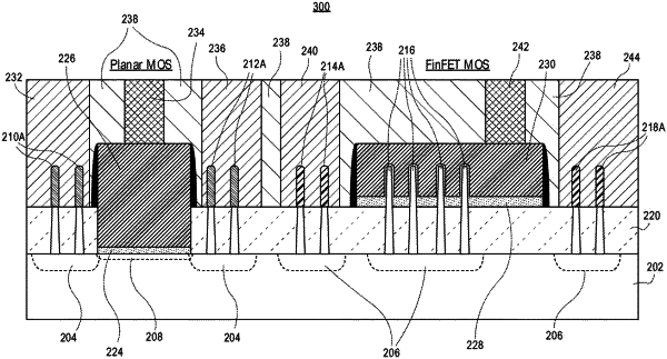
1. An integrated circuit structure, comprising:
a first fin structure and a second fin structure protruding through a dielectric layer above a semiconductor substrate, the dielectric layer having an uppermost surface;
a gate structure directly on a portion of the semiconductor substrate, the portion of the semiconductor substrate between the first fin structure and the second fin structure, the gate structure comprising a gate electrode having a bottommost surface below the uppermost surface of the dielectric layer;
a source region in the first fin structure; and
a drain region in the second fin structure.
|
|
10. An integrated circuit structure, comprising:
a buried channel device, comprising:
a source region in a first fin structure protruding through a dielectric layer above a semiconductor substrate, the dielectric layer having an uppermost surface;
a drain region in a second fin structure protruding through the dielectric layer above the semiconductor substrate; and
a first gate structure between the source region and the drain region, the first gate structure directly on a substantially planar region of the semiconductor substrate between the first fin structure and the second fin structure, the gate structure comprising a gate electrode having a bottommost surface below the uppermost surface of the dielectric layer; and
a non-planar device comprising a second gate structure over a plurality of fins above the semiconductor substrate.
|
|
13. A computing device, comprising:
a board; and
a component coupled to the board, the component including an integrated circuit structure, comprising:
a first fin structure and a second fin structure protruding through a dielectric layer above a semiconductor substrate, the dielectric layer having an uppermost surface;
a gate structure directly on a portion of the semiconductor substrate, the portion of the semiconductor substrate between the first fin structure and the second fin structure, the gate structure comprising a gate electrode having a bottommost surface below the uppermost surface of the dielectric layer;
a source region in the first fin structure; and
a drain region in the second fin structure.
|