| CPC H01L 27/0255 (2013.01) [H01L 21/74 (2013.01); H01L 23/562 (2013.01); H01L 28/90 (2013.01)] | 14 Claims |
|
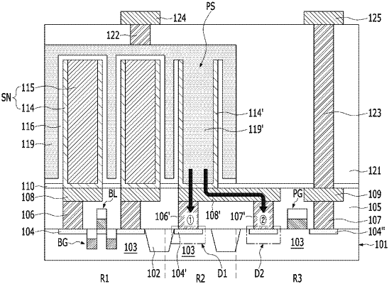
1. A semiconductor device, comprising:
a capacitor disposed over a substrate and including a lower electrode, a dielectric layer and an upper electrode; and
a discharge structure spaced apart from the capacitor, connected to the upper electrode of the capacitor and suitable for discharging, to the substrate, a charge induced from a plasma process for forming the upper electrode of the capacitor,
wherein the discharge structure includes:
a second electrode;
a first electrode connected to the second electrode;
a discharge contact plug connected to the first electrode; and
a diode connected to the discharge contact plug and formed in the substrate,
wherein the discharge contact plug further includes:
a first discharge contact plug connected to the diode; and
a second discharge contact plug of which both ends are connected respectively to the first discharge contact plug and the first electrode.
|