| CPC H01L 25/18 (2013.01) [H01L 23/3128 (2013.01); H01L 23/49816 (2013.01); H01L 23/49822 (2013.01); H01L 23/49833 (2013.01); H01L 23/49838 (2013.01); H01L 23/5385 (2013.01); H01L 23/5386 (2013.01); H01L 24/06 (2013.01); H01L 24/73 (2013.01); H01L 2224/0401 (2013.01); H01L 2224/06515 (2013.01); H01L 2224/16146 (2013.01); H01L 2224/16148 (2013.01); H01L 2224/16235 (2013.01); H01L 2224/16238 (2013.01); H01L 2224/73204 (2013.01); H01L 2924/1431 (2013.01); H01L 2924/1434 (2013.01); H01L 2924/3511 (2013.01)] | 20 Claims |
|
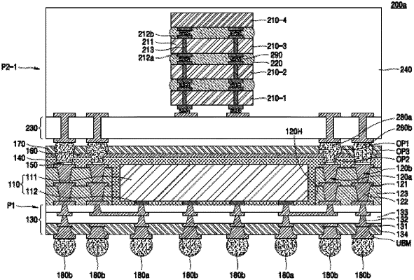
1. A semiconductor package, comprising:
a package substrate;
a first bump and a second bump on a lower surface of the package substrate;
a semiconductor chip on an upper surface of the package substrate;
a first connection pattern and a second connection pattern on the upper surface of the package substrate;
a molding on the upper surface of the package substrate, the molding covering the semiconductor chip;
a warpage control layer on the molding;
an upper insulating layer on the warpage control layer;
a first opening passing through the upper insulating layer and exposing an upper surface of the warpage control layer;
a second opening overlapping the first opening in a top view, the second opening passing through the warpage control layer and exposing the first connection pattern; and
a third opening passing through the upper insulating layer and exposing the second connection pattern.
|