US 11,728,322 B2
Photosensitive imaging devices and associated methods
Jutao Jiang, Tigard, OR (US); Jeffrey McKee, Tualatin, OR (US); and Martin U. Pralle, Wayland, MA (US)
Assigned to SIONYX, LLC, Beverly, MA (US)
Filed by SiOnyx, LLC, Beverly, MA (US)
Filed on Feb. 25, 2022, as Appl. No. 17/681,252.
Application 17/681,252 is a continuation of application No. 16/945,136, filed on Jul. 31, 2020, granted, now 11,264,371.
Application 16/945,136 is a continuation of application No. 16/290,756, filed on Mar. 1, 2019, granted, now 10,748,956, issued on Aug. 18, 2020.
Application 16/290,756 is a continuation of application No. 15/674,136, filed on Aug. 10, 2017, granted, now 10,229,951, issued on Mar. 12, 2019.
Application 15/674,136 is a continuation of application No. 14/245,872, filed on Apr. 4, 2014, granted, now 9,741,761, issued on Aug. 22, 2017.
Application 14/245,872 is a continuation of application No. 13/091,969, filed on Apr. 21, 2011, granted, now 8,692,198, issued on Apr. 18, 2014.
Claims priority of provisional application 61/326,489, filed on Apr. 21, 2010.
Prior Publication US 2022/0359481 A1, Nov. 10, 2022
Int. Cl. H01L 25/16 (2023.01); H01L 27/146 (2006.01); H04N 23/56 (2023.01); H04N 25/70 (2023.01); H04N 25/71 (2023.01); H04N 25/771 (2023.01); H04N 25/131 (2023.01); H04N 25/13 (2023.01)
CPC H01L 25/167 (2013.01) [H01L 27/1461 (2013.01); H01L 27/1464 (2013.01); H01L 27/14612 (2013.01); H01L 27/14625 (2013.01); H01L 27/14645 (2013.01); H01L 27/14647 (2013.01); H01L 27/14649 (2013.01); H04N 23/56 (2023.01); H04N 25/70 (2023.01); H04N 25/745 (2023.01); H04N 25/771 (2023.01); H01L 2924/0002 (2013.01); H04N 25/131 (2023.01); H04N 25/135 (2023.01)] 10 Claims
OG exemplary drawing
 
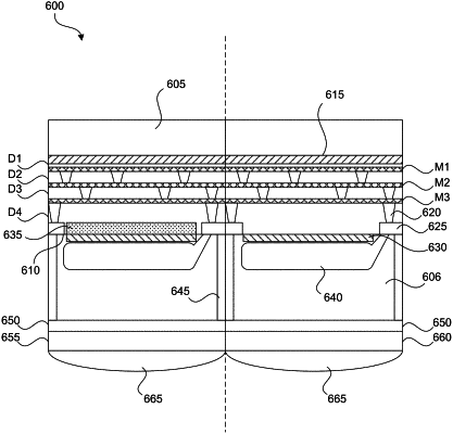
1. A monolithic sensor for detecting infrared and visible light, comprising:
a semiconductor substrate;
a semiconductor layer coupled to the semiconductor substrate, the semiconductor layer having a device surface opposite the semiconductor substrate;
a visible light photodiode formed at the device surface;
an infrared photodiode formed at the device surface in proximity to the visible light photodiode; and
a light diffusing region coupled to the infrared photodiode and positioned to interact with electromagnetic radiation.