| CPC H01L 25/105 (2013.01) [H01L 21/561 (2013.01); H01L 23/3128 (2013.01); H01L 25/18 (2013.01); H01L 23/295 (2013.01); H01L 24/16 (2013.01); H01L 24/48 (2013.01); H01L 24/73 (2013.01); H01L 2224/16227 (2013.01); H01L 2224/48227 (2013.01); H01L 2224/73204 (2013.01); H01L 2225/1023 (2013.01); H01L 2225/1041 (2013.01); H01L 2225/1058 (2013.01); H01L 2924/19041 (2013.01); H01L 2924/19106 (2013.01)] | 20 Claims |
|
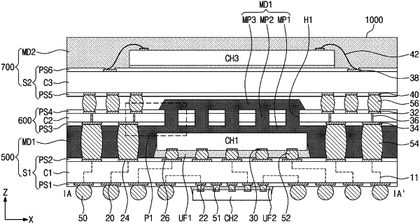
1. A semiconductor package, comprising:
a first sub-semiconductor package, an interposer substrate, and a second sub-semiconductor package that are sequentially stacked,
wherein the first sub-semiconductor package comprises a first package substrate, a first semiconductor device, and a first mold member that are sequentially stacked,
the interposer substrate comprises at least one hole,
the first mold member comprises:
a mold main portion which covers the first semiconductor device;
a mold connecting portion extended from the mold main portion and inserted into the at least one hole; and
a mold protruding portion extended from the mold connecting portion to cover a top surface of the interposer substrate outside the at least one hole, and
the mold main portion, the mold connecting portion, and the mold protruding portion constitute a single object.
|