| CPC H01L 25/0657 (2013.01) [H01L 21/486 (2013.01); H01L 23/49827 (2013.01); H01L 25/18 (2013.01); H01L 25/50 (2013.01); H01L 2225/06524 (2013.01); H01L 2225/06541 (2013.01); H01L 2225/06589 (2013.01)] | 19 Claims |
|
1. A method for fabricating a semiconductor device, comprising:
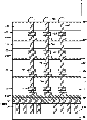
forming a carrier substrate;
forming a plurality of substrate vias in the carrier substrate for thermally conducting heat;
forming a carrier bonding layer on the carrier substrate, wherein the carrier substrate, the plurality of substrate vias, and the carrier bonding layer together configure a carrier structure;
providing a first die structure comprising a plurality of through semiconductor vias;
forming an intervening bonding layer on the first die structure;
bonding the first die structure onto the carrier bonding layer of the carrier structure through the intervening bonding layer; and
bonding a second die structure onto the first die structure, wherein the second die structure and the first die structure are electrically coupled by the plurality of through semiconductor vias.
|