| CPC H01L 25/0652 (2013.01) [H01L 23/481 (2013.01); H01L 23/49816 (2013.01); H01L 23/5223 (2013.01); H01L 23/5286 (2013.01); H01L 23/642 (2013.01)] | 20 Claims |
|
1. A semiconductor device, comprising:
an interposer substrate; and
at least one die mounted on the interposer substrate,
wherein the interposer substrate includes
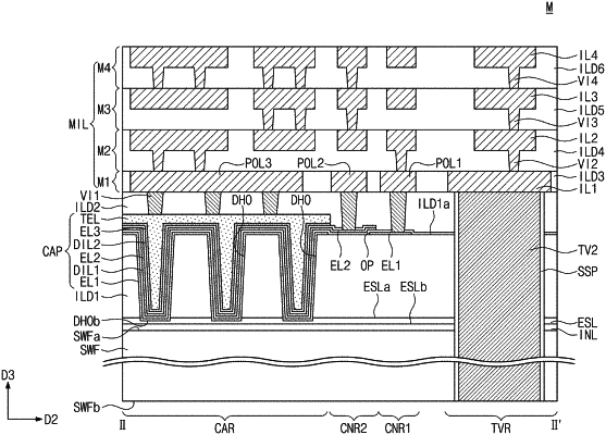
a semiconductor substrate having a first surface and a second surface opposite to the first surface,
an interlayer insulating layer on the first surface of the semiconductor substrate,
a capacitor in a hole penetrating the interlayer insulating layer,
an interconnection layer on the interlayer insulating layer, and
a through-via extending from the interconnection layer toward the second surface of the semiconductor substrate in a vertical direction that is perpendicular to the first surface of the semiconductor substrate,
wherein the hold penetrating the interlayer insulating layer extends in the vertical direction and includes sidewalls at least partially defined by an inner sidewall surface and a bottom surface,
wherein the capacitor includes a sequential stack, of a first electrode, a first dielectric layer, a second electrode, a second dielectric layer, and a third electrode, that is at least partially in the hole penetrating the interlayer insulating layer and extending along the inner sidewall surface and the bottom surface of the hole penetrating the interlayer insulating layer, and
wherein the capacitor is spaced apart from the semiconductor substrate, such that a bottom of the hole is distal from the second surface of the semiconductor substrate in relation to the first surface of the semiconductor substrate and the first surface of the semiconductor substrate is between the bottom of the hole and the second surface of the semiconductor substrate.
|