| CPC H01L 24/81 (2013.01) [B23K 26/22 (2013.01); H01L 23/49866 (2013.01); H01L 24/83 (2013.01); H01L 25/0753 (2013.01); H01L 25/167 (2013.01); B23K 2101/40 (2018.08); H01L 2224/81005 (2013.01); H01L 2224/81224 (2013.01); H01L 2224/83005 (2013.01); H01L 2224/83224 (2013.01); H01L 2924/12041 (2013.01)] | 10 Claims |
|
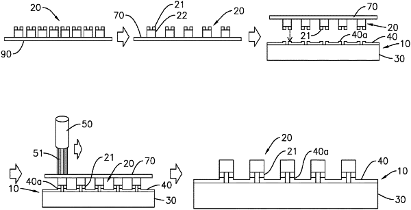
1. A method of manufacturing a lighting device, comprising:
providing a circuit structure, the circuit structure comprising a glass plate and a first electrical contact arranged on the glass plate;
providing a first semiconductor element, a second semiconductor element, and a third semiconductor element, the first semiconductor element having a first electrode;
applying a first bonding material;
arranging the first semiconductor element, the second semiconductor element, and the third semiconductor element on the circuit structure, the first electrode being aligned with and facing to the first electrical contact; and
providing an energy beam in a dot-scattering heating pattern to heat the first bonding material and join the first electrode and the first electrical contract.
|