| CPC H01L 24/13 (2013.01) [H01L 24/11 (2013.01); H01L 2224/1147 (2013.01); H01L 2224/13013 (2013.01); H01L 2224/13014 (2013.01); H01L 2224/13078 (2013.01); H01L 2224/13147 (2013.01); H01L 2224/13155 (2013.01); H01L 2924/3512 (2013.01)] | 21 Claims |
|
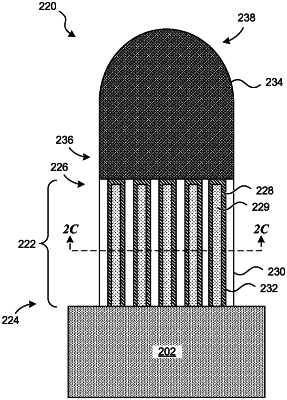
1. A semiconductor device, comprising:
a semiconductor die; and
a pillar structure coupled to the semiconductor die, wherein the pillar structure includes—
a plurality of conductive elements, each electrically coupled to and extending linearly away from the semiconductor die, wherein each conductive element includes a first conductive material having a first elastic modulus, and
a continuous region of a second conductive material at least partially surrounding the plurality of conductive elements, the second conductive material having a second elastic modulus less than the first elastic modulus.
|