| CPC H01L 24/08 (2013.01) [H01L 24/80 (2013.01); H01L 25/0657 (2013.01); H01L 25/18 (2013.01); H01L 25/50 (2013.01); H01L 28/60 (2013.01); H01L 2224/08145 (2013.01); H01L 2224/80895 (2013.01); H01L 2224/80896 (2013.01); H01L 2924/1431 (2013.01); H01L 2924/1434 (2013.01); H01L 2924/19041 (2013.01); H01L 2924/19104 (2013.01)] | 14 Claims |

|
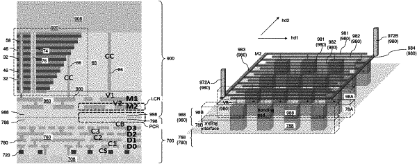
1. A semiconductor structure, comprising:
a bonded assembly of a first semiconductor die including first metal bonding pads and a second semiconductor die including second metal bonding pads that are bonded to the first metal bonding pads; and
a capacitor structure comprising a first electrode, a second electrode, and a node dielectric disposed between the first electrode and the second electrode,
wherein:
the first electrode comprises first bonded pairs of a respective first metal bonding pad of a first subset of the first metal bonding pads and a respective second metal bonding pad of a first subset of the second metal bonding pads;
the second electrode comprises second bonded pairs of a respective first metal bonding pad of a second subset of the first metal bonding pads and a respective second metal bonding pad of a second subset of the second metal bonding pads;
the node dielectric comprises portions of a first bonding-level dielectric layer laterally surrounding the first metal bonding pads and disposed between laterally neighboring pairs of the first metal bonding pads and portions of a second bonding-level dielectric layer laterally surrounding the second metal bonding pads and disposed between laterally neighboring pairs of the second metal bonding pads;
the first subset of the first metal bonding pads, the first subset of the second metal bonding pads, the second subset of the first metal bonding pads, and the second subset of the second metal bonding pads comprise respective rows of metal bonding pads having a periodic pitch along a first horizontal direction and having a nearest-neighbor spacing within each row that is less than one half of the periodic pitch along the first horizontal direction; and
the periodic pitch is in a range from 1,000 nm to 10,000 nm.
|