| CPC H01L 24/06 (2013.01) [H01L 23/5226 (2013.01); H01L 23/5286 (2013.01); H01L 2224/02331 (2013.01); H01L 2224/02373 (2013.01); H01L 2224/0401 (2013.01); H01L 2224/06131 (2013.01); H01L 2224/06177 (2013.01)] | 19 Claims |
|
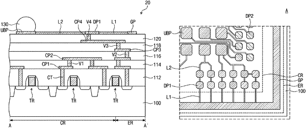
1. A semiconductor device comprising:
a semiconductor substrate;
at least one integrated device on a front surface of the semiconductor substrate;
a first redistribution layer on the semiconductor substrate, the first redistribution layer having a plurality of first conductive patterns electrically connected to the at least one integrated device;
a second redistribution layer on the first redistribution layer, the second redistribution layer having a plurality of second conductive patterns connected to the plurality of first conductive patterns; and
a plurality of third conductive patterns on a top surface of the second redistribution layer,
wherein the plurality of third conductive patterns include:
a plurality of pads connected to the plurality of second conductive patterns;
a plurality of under-bump pads spaced apart from the plurality of pads;
a grouping pattern between the plurality of pads and an outer edge of the second redistribution layer; and
a plurality of wiring lines that connect the plurality of under-bump pads to the plurality of pads and connect the plurality of pads to the grouping pattern,
wherein the plurality of pads, the plurality of under-bump pads, the grouping pattern, and the plurality of wiring lines are located at the same level from the semiconductor substrate.
|