| CPC H01L 24/05 (2013.01) [H01L 21/76867 (2013.01); H01L 23/3107 (2013.01); H01L 23/4952 (2013.01); H01L 23/49548 (2013.01); H01L 23/49562 (2013.01); H01L 23/49582 (2013.01); H01L 24/29 (2013.01); H01L 24/46 (2013.01); H01L 24/49 (2013.01); H01L 24/97 (2013.01); H01L 23/562 (2013.01); H01L 24/06 (2013.01); H01L 24/32 (2013.01); H01L 24/48 (2013.01); H01L 2224/04026 (2013.01); H01L 2224/04042 (2013.01); H01L 2224/05553 (2013.01); H01L 2224/05554 (2013.01); H01L 2224/0603 (2013.01); H01L 2224/29644 (2013.01); H01L 2224/32245 (2013.01); H01L 2224/48247 (2013.01); H01L 2224/48465 (2013.01); H01L 2224/49111 (2013.01); H01L 2224/49113 (2013.01); H01L 2224/49431 (2013.01); H01L 2224/73265 (2013.01); H01L 2224/97 (2013.01); H01L 2924/00014 (2013.01); H01L 2924/15747 (2013.01); H01L 2924/181 (2013.01)] | 20 Claims |
|
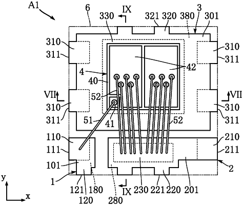
1. A semiconductor device comprising:
a first lead having an obverse surface and a reverse surface that are spaced apart from each other in a thickness direction;
a semiconductor element provided with at least one electrode and supported by the first lead;
a second lead adjacent to the first lead;
a third lead adjacent to the first lead;
a sealing resin covering a part of the first lead, a part of the second lead, a part of the third lead, and the semiconductor element, the sealing resin being rectangular in plan view and including a first side surface, a second side surface opposite to the first side surface, a third side surface other than the first and the second side surface, and a bottom surface;
a first wire connecting the semiconductor element to the second lead; and
a second wire connecting the semiconductor element to the third lead,
wherein the first lead comprises an exposed portion that is exposed from the bottom surface of the sealing resin,
the second lead includes a first exposed portion exposed from the first side surface of the sealing resin,
the third lead includes a second exposed portion exposed from the second side surface of the sealing resin,
the first and second side surfaces of the sealing resin each include a first section and a second section, the first section being disposed outward with respect to the second section in plan view, the first exposed portion being located in the second section of the first side surface of the sealing resin, the second exposed portion being located in the second section of the second side surface of the sealing resin, wherein the second exposed portion and the second section of the second side surface have respective regions that are flush with each other.
|