| CPC H01L 24/05 (2013.01) [H01L 23/3135 (2013.01); H01L 23/3171 (2013.01); H01L 23/481 (2013.01); H01L 24/03 (2013.01); H01L 24/13 (2013.01); H01L 24/16 (2013.01); H01L 25/0657 (2013.01); H01L 23/3128 (2013.01); H01L 24/17 (2013.01); H01L 24/32 (2013.01); H01L 24/73 (2013.01); H01L 24/81 (2013.01); H01L 24/92 (2013.01); H01L 25/18 (2013.01); H01L 2224/0362 (2013.01); H01L 2224/03416 (2013.01); H01L 2224/03418 (2013.01); H01L 2224/03452 (2013.01); H01L 2224/03462 (2013.01); H01L 2224/03464 (2013.01); H01L 2224/03614 (2013.01); H01L 2224/03831 (2013.01); H01L 2224/03916 (2013.01); H01L 2224/0401 (2013.01); H01L 2224/0508 (2013.01); H01L 2224/05016 (2013.01); H01L 2224/05017 (2013.01); H01L 2224/05022 (2013.01); H01L 2224/05024 (2013.01); H01L 2224/05085 (2013.01); H01L 2224/05124 (2013.01); H01L 2224/05144 (2013.01); H01L 2224/05147 (2013.01); H01L 2224/05155 (2013.01); H01L 2224/05164 (2013.01); H01L 2224/05166 (2013.01); H01L 2224/05169 (2013.01); H01L 2224/05171 (2013.01); H01L 2224/05181 (2013.01); H01L 2224/05184 (2013.01); H01L 2224/05557 (2013.01); H01L 2224/05558 (2013.01); H01L 2224/05562 (2013.01); H01L 2224/05564 (2013.01); H01L 2224/05567 (2013.01); H01L 2224/05568 (2013.01); H01L 2224/05582 (2013.01); H01L 2224/05624 (2013.01); H01L 2224/05639 (2013.01); H01L 2224/05644 (2013.01); H01L 2224/05647 (2013.01); H01L 2224/05655 (2013.01); H01L 2224/05669 (2013.01); H01L 2224/05684 (2013.01); H01L 2224/06181 (2013.01); H01L 2224/1312 (2013.01); H01L 2224/13022 (2013.01); H01L 2224/13024 (2013.01); H01L 2224/13025 (2013.01); H01L 2224/13082 (2013.01); H01L 2224/13109 (2013.01); H01L 2224/13111 (2013.01); H01L 2224/13113 (2013.01); H01L 2224/13116 (2013.01); H01L 2224/13118 (2013.01); H01L 2224/13139 (2013.01); H01L 2224/13144 (2013.01); H01L 2224/13147 (2013.01); H01L 2224/13155 (2013.01); H01L 2224/13164 (2013.01); H01L 2224/13169 (2013.01); H01L 2224/16145 (2013.01); H01L 2224/16148 (2013.01); H01L 2224/16227 (2013.01); H01L 2224/17181 (2013.01); H01L 2224/32145 (2013.01); H01L 2224/32225 (2013.01); H01L 2224/73204 (2013.01); H01L 2224/8181 (2013.01); H01L 2224/81203 (2013.01); H01L 2224/81815 (2013.01); H01L 2224/92125 (2013.01); H01L 2225/06513 (2013.01); H01L 2225/06517 (2013.01); H01L 2225/06541 (2013.01); H01L 2225/06586 (2013.01); H01L 2924/04941 (2013.01); H01L 2924/04953 (2013.01); H01L 2924/15311 (2013.01)] | 20 Claims |

|
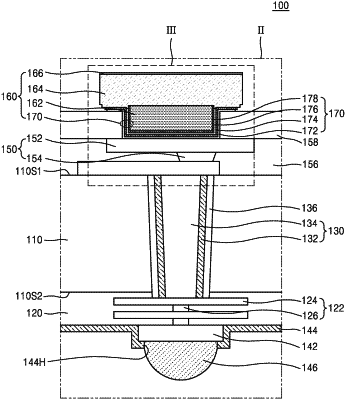
1. A method of manufacturing a semiconductor device, the method comprising:
forming, on a substrate, a passivation layer comprising an opening therein, the opening exposing at least a portion of a conductive component;
forming a lower conductive layer on an inner sidewall of the opening and a top surface of the passivation layer by sequentially forming a conductive barrier layer, a first seed layer, an etch stop layer, and a second seed layer;
forming a mold layer on the lower conductive layer, the mold layer comprising a pad space communicated with the opening;
forming, on the lower conductive layer, a first pad layer in the opening and the pad space by using the second seed layer as a seed material, and etching back an upper portion of the first pad layer until a top surface of the etch stop layer is exposed, such that the first pad layer fills only the opening; and
forming, on the first pad layer, a second pad layer in the pad space.
|