| CPC H01L 24/03 (2013.01) [H01L 24/05 (2013.01); H01L 24/13 (2013.01); H01L 2224/0239 (2013.01); H01L 2224/02311 (2013.01); H01L 2224/02313 (2013.01); H01L 2224/02331 (2013.01); H01L 2224/0401 (2013.01); H01L 2224/13144 (2013.01); H01L 2224/13147 (2013.01); H01L 2924/01027 (2013.01); H01L 2924/01029 (2013.01)] | 20 Claims |
|
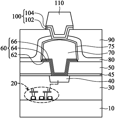
1. A method of manufacturing a semiconductor device, comprising:
forming an opening in a first dielectric layer so that a part of a lower conductive layer is exposed at a bottom of the opening;
forming one or more liner conductive layers over the part of the lower conductive layer, an inner sidewall of the opening and an upper surface of the first dielectric layer;
forming a main conductive layer over the one or more liner conductive layers;
forming a patterned conductive layer by patterning the main conductive layer and the one or more liner conductive layers using lithography and etching operations; and
forming a cover conductive layer over the patterned conductive layer,
wherein the main conductive layer which is patterned is wrapped around by the cover conductive layer and one of the one or more liner conductive layers.
|