| CPC H01L 23/66 (2013.01) [H01L 21/486 (2013.01); H01L 21/4857 (2013.01); H01L 21/6835 (2013.01); H01L 23/5386 (2013.01); H01L 24/16 (2013.01); H01L 25/0655 (2013.01); H01L 25/50 (2013.01); H01L 24/97 (2013.01); H01L 2221/68345 (2013.01); H01L 2221/68359 (2013.01); H01L 2223/6616 (2013.01); H01L 2223/6627 (2013.01); H01L 2223/6683 (2013.01); H01L 2224/16227 (2013.01); H01L 2924/1423 (2013.01); H01L 2924/1903 (2013.01)] | 12 Claims |
|
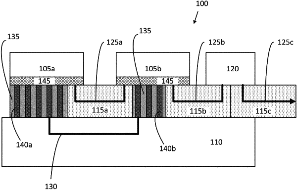
1. A microelectronic package comprising:
a package substrate that includes a face and a substrate signal path, wherein the substrate signal path is positioned between two dielectric layers of the package substrate;
a first die and a second die coupled with the package substrate and communicatively coupled with the substrate signal path; and
a waveguide coupled with the face of the package substrate, wherein the waveguide is communicatively coupled with the first die and the second die;
wherein the waveguide is to carry an electromagnetic signal with a first frequency from the first die to the second die, and the substrate signal path is to carry an electromagnetic signal with a second frequency from the first die to the second die, and wherein the first frequency is greater than the second frequency.
|