| CPC H01L 23/562 (2013.01) [H01L 21/31144 (2013.01); H01L 21/76802 (2013.01); H01L 21/76877 (2013.01); H01L 21/78 (2013.01)] | 9 Claims |
|
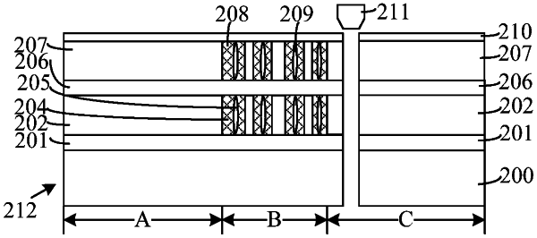
1. A semiconductor structure, comprising:
a wafer having a functional region and a non-functional region surrounding the functional region;
a first dielectric layer formed on the wafer;
a first opening formed in the first dielectric layer on the non-function region of the wafer; and
a first connection layer formed in the first opening,
wherein the first connection layer closes a top portion of the first opening and a first void is formed in the first connection layer in the first opening.
|