| CPC H01L 23/562 (2013.01) [H01L 23/3128 (2013.01); H01L 23/5383 (2013.01); H01L 23/5386 (2013.01); H01L 23/5389 (2013.01); H01L 23/64 (2013.01); H01L 24/20 (2013.01); H01L 25/105 (2013.01); H01L 2224/214 (2013.01); H01L 2225/1035 (2013.01); H01L 2225/1058 (2013.01); H01L 2924/30111 (2013.01); H01L 2924/3511 (2013.01)] | 18 Claims |
|
1. A semiconductor package comprising:
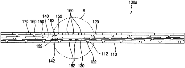
a package substrate including a first insulation layer, first redistribution layers (RDL), a second insulation layer, second RDLs, a third insulation layer, third RDLs, a pair of impedance patterns, and a fourth insulation layer, the first insulation layer including a plurality of first via holes, the first RDLs arranged on an upper surface of the first insulation layer to fill the first via holes, the second insulation layer arranged on an upper surface of the first insulation layer and including a plurality of second via holes configured to expose the first RDLs, the second RDLs arranged on an upper surface of the second insulation layer and in the second via holes to be electrically connected with the first RDLs, the third insulation layer arranged on an upper surface of the second insulation layer and having a plurality of third via holes configured to expose the second RDLs, the third RDLs arranged on an upper surface of the third insulation layer and in the third via holes to be electrically connected with the second RDLs, the pair of impedance patterns arranged on the upper surface of the third insulation layer over the second RDLs, the pair of impedance patterns having an insulation length corresponding to a summed length of a thickness of the second insulation layer and a thickness of the third insulation layer, and the fourth insulation layer arranged on the upper surface of the third insulation layer to surround the third RDLs and the impedance patterns;
a semiconductor chip arranged on an upper surface of the package substrate and electrically connected with the third RDLs;
a molding member arranged on the upper surface of the package substrate to surround the semiconductor chip; and
external terminals arranged on a lower surface of the package substrate and electrically connected with the first RDLs,
wherein the pair of impedance patterns are positioned on a horizontal plane under a horizontal plane on which the third RDLs are placed.
|