| CPC H01L 23/552 (2013.01) [H01L 21/4814 (2013.01); H01L 21/4853 (2013.01); H01L 21/563 (2013.01); H01L 23/3121 (2013.01); H01R 12/52 (2013.01); H01R 12/79 (2013.01); H01R 43/205 (2013.01); H01R 43/26 (2013.01); H01L 21/565 (2013.01)] | 25 Claims |

|
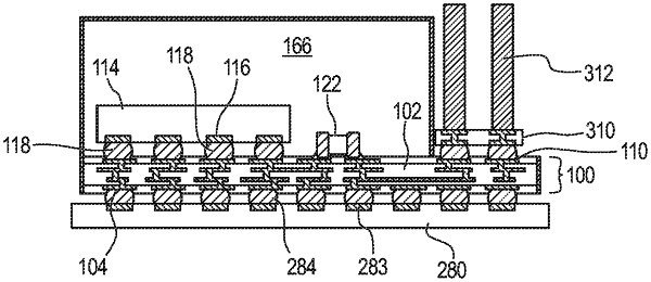
1. A semiconductor device, comprising:
a substrate;
a terminal formed over the substrate;
an insulating layer formed over the substrate including an opening in the insulating layer over the terminal;
an encapsulant disposed over a first portion of the insulating layer while a second portion of the insulating layer around the opening of the insulating layer remains exposed from the encapsulant; and
a shielding layer formed over the substrate, insulating layer, and encapsulant with the shielding layer physically contacting the second portion of the insulating layer, wherein an opening in the shielding layer is formed over the terminal.
|